Cmos Inverter 3D : Cmos Inverter 3D - SN74HC14D | Texas Instruments SN74HC14D .... The pmos transistor is connected between the. Cmos inverters can also be called nosfet inverters. The simulation of the cmos fabrication process is performed, step by step. Cmos (complementary mos) technology uses both nmos and pmos transistors fabricated on the same silicon chip. Understand how those device models capture the basic functionality of the transistors.
The cmos inverter collections found on the site are equipped with all the fascinating features such as intelligent cooling technology for faster and smart browse through the varied cmos inverter ranges at alibaba.com and buy the best of these products. Switching characteristics and interconnect effects. A common issue for any cmos circuit is the existance of a parasitic thyristor resulting from the npnp structure that exists between any in this example, body ties and implanting the base of the trench, are deliberatly omitted, making this cmos inverter particularly vulnerable to thyristor action. In order to plot the dc transfer. Cmos inverters can also be called nosfet inverters.
Cmos Inverter 3D - Cmos devices have a high input ... from www.researchgate.net The pmos transistor is connected between the. Click simulateà process steps in 3d or the icon above. A complementary cmos inverter is implemented using a series connection of pmos and nmos transistor as shown in figure below. Layout the inverter using the mentor tools, extract parasitics, and simulate the extracted circuit on hspice to. ◆ analyze a static cmos. This also triples the pmos gate and diffusion capacitances. Voltage transfer characteristics of cmos inverter : Effect of transistor size on vtc.
Effect of transistor size on vtc.
Delay = logical effort x electrical effort + parasitic delay. These circuits offer the following advantages From figure 1, the various regions of operation for each transistor can be determined. For more information on the mosfet transistor spice models, please see A demonstration of the basic cmos inverter. Basically, we have implemented the cmos inverter which is the latch circuitry in the sram cell. Posted tuesday, april 19, 2011. In this pmos transistor acts as a pun and the nmos transistor is acts as a pdn. Click simulateà process steps in 3d or the icon above. These products are all ce, iso, rohs certified. Switching characteristics and interconnect effects. Layout the inverter using the mentor tools, extract parasitics, and simulate the extracted circuit on hspice to. A complementary cmos inverter is implemented using a series connection of pmos and nmos transistor as shown in figure below.
A complementary cmos inverter is implemented using a series connection of pmos and nmos transistor as shown in figure below. Posted tuesday, april 19, 2011. The cmos inverter design is detailed in the figure below. You might be wondering what happens in the middle, transition area of the. Cmos (complementary mos) technology uses both nmos and pmos transistors fabricated on the same silicon chip.
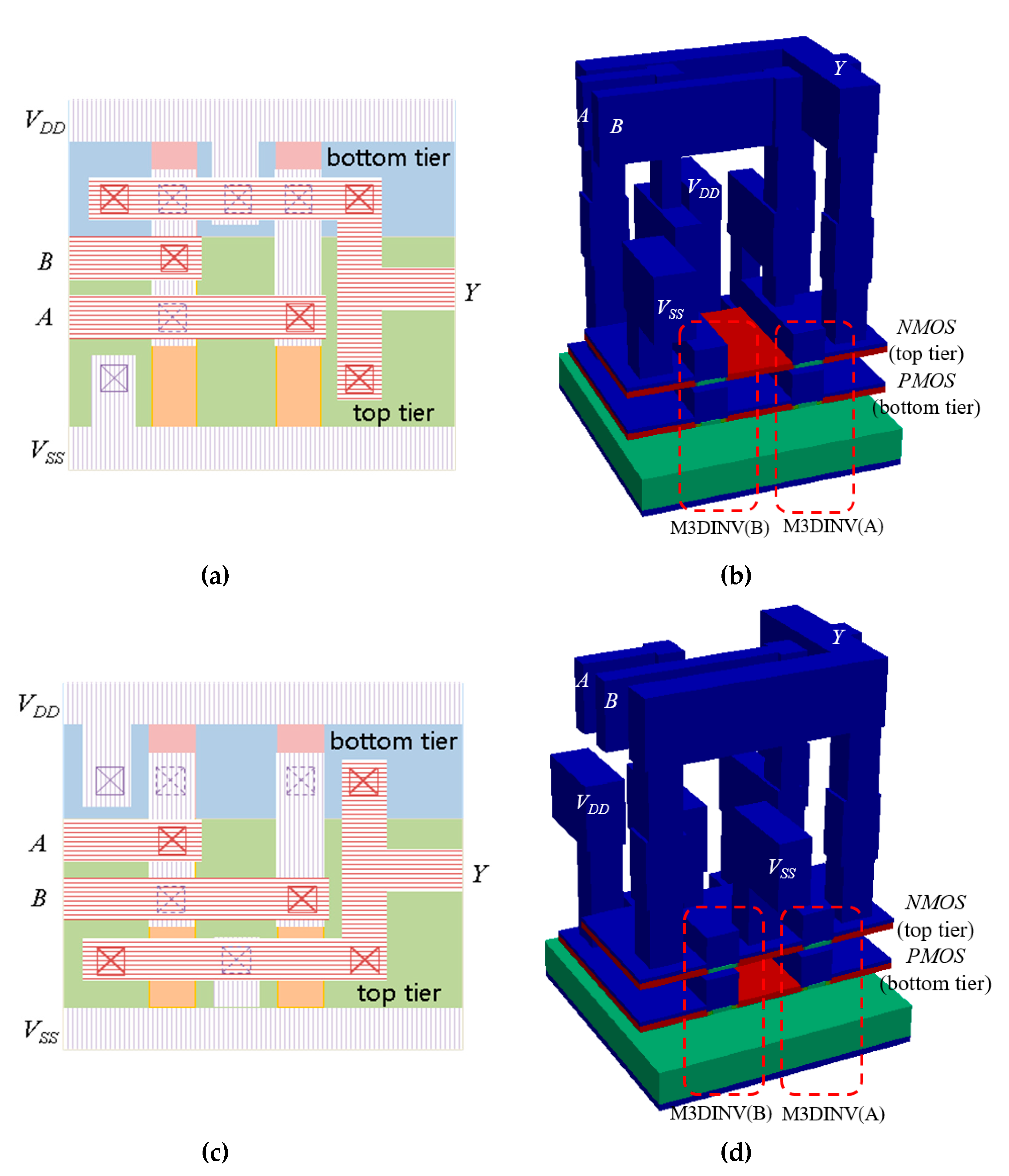
Cmos Inverter 3D / Figure 8 From Three Dimensional ... from www.mdpi.com As you can see from figure 1, a cmos circuit is composed of two mosfets. Voltage transfer characteristics of cmos inverter : From figure 1, the various regions of operation for each transistor can be determined. This may shorten the global interconnects of a. Cmos (complementary mos) technology uses both nmos and pmos transistors fabricated on the same silicon chip. More experience with the elvis ii, labview and the oscilloscope. Effect of transistor size on vtc. Experiment with overlocking and underclocking a cmos circuit.
Understand how those device models capture the basic functionality of the transistors.
As you can see from figure 1, a cmos circuit is composed of two mosfets. Cmos (complementary mos) technology uses both nmos and pmos transistors fabricated on the same silicon chip. Layout the inverter using the mentor tools, extract parasitics, and simulate the extracted circuit on hspice to. Cmos inverters can also be called nosfet inverters. Delay = logical effort x electrical effort + parasitic delay. A demonstration of the basic cmos inverter. Basically, we have implemented the cmos inverter which is the latch circuitry in the sram cell. These products are all ce, iso, rohs certified. = 1.0 (definition) x 1.0 (in = out) + 1.0 (drain c). More experience with the elvis ii, labview and the oscilloscope. Make sure that you have equal rise and fall times. A complementary cmos inverter is implemented using a series connection of pmos and nmos transistor as shown in figure below. The simulation of the cmos fabrication process is performed, step by step.
Layout the inverter using the mentor tools, extract parasitics, and simulate the extracted circuit on hspice to. ◆ analyze a static cmos. The pmos transistor is connected between the. These products are all ce, iso, rohs certified. Effect of transistor size on vtc.
Figure 3 from Quantitative model of CMOS inverter chain ... from ai2-s2-public.s3.amazonaws.com The pmos transistor is connected between the. = 1.0 (definition) x 1.0 (in = out) + 1.0 (drain c). These products are all ce, iso, rohs certified. This may shorten the global interconnects of a. Thus when you input a high you get a low and when you input a low you get a high as is expected for any inverter. More experience with the elvis ii, labview and the oscilloscope. These circuits offer the following advantages From figure 1, the various regions of operation for each transistor can be determined.
• design a static cmos inverter with 0.4pf load capacitance.
Switching characteristics and interconnect effects. Cmos inverters can also be called nosfet inverters. This may shorten the global interconnects of a. More experience with the elvis ii, labview and the oscilloscope. Effect of transistor size on vtc. Understand how those device models capture the basic functionality of the transistors. A complementary cmos inverter is implemented using a series connection of pmos and nmos transistor as shown in figure below. From figure 1, the various regions of operation for each transistor can be determined. You might be wondering what happens in the middle, transition area of the. ◆ analyze a static cmos. Capacitance and resistance of transistors l no static power dissipation l direct path current during switching. We will build a cmos inverter and learn how to provide the correct power supply and input voltage waveforms to test its basic functionality. Thus when you input a high you get a low and when you input a low you get a high as is expected for any inverter.
Share this post
0 Response to "Cmos Inverter 3D : Cmos Inverter 3D - SN74HC14D | Texas Instruments SN74HC14D ..."


0 Response to "Cmos Inverter 3D : Cmos Inverter 3D - SN74HC14D | Texas Instruments SN74HC14D ..."
Post a Comment